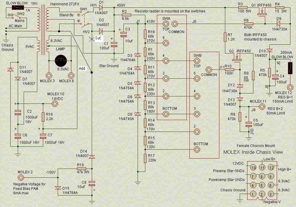
The power supply is very flexible, generatint two independent, variable B+ voltages. The preamp B+ is 50mA, current limited, with six output voltages: 120; 160; 200; 240; 280 and 320V. The power amp supply is 150mA, fuse protected, with six output voltages: 200; 240; 280; 320; 360 and 400V. Both are series regulated, well filtered, "stiff" sources of high voltage. Output impedance is ~130 ohms.
UPDATE 4/22/2002: An error was found. The negative voltage must remain powered in stand by. The fix is hand edited into the schematic. A fix for the PCB is shown on the PSM PCB page.
Contents

Theory of Operation
The PSM is very straight forward, intended to be cheap and simple enough for any tube amp hobbyist. The Hammond 272FX PT was chosen at a "cost optimal" point to provide capability up to a push-pull EL34 or 6L6 style power amp up to ~50W. Rectification is solid state to get the maximum voltage with as little sag as possible. Series regulation is done with IRFP450 power MOSFETs. These devices are cheap and easily handle tube amp currents and voltages. In fact, these devices can provide regulation superior to choke and capacitance regulation with the added benefit of voltage variability. As such, there is no choke in the PSM. Variability is provided via two independent 6-position switches. These switches select a voltage tapped off a resistor divider to bias the MOSFET gates. Finally, current is limited via a current sensing resistor on the source of the MOSFETs. The pre-amp supply is limited to 50mA and the power-amp supply is limited to 180mA (in addition to being fused for short circuit protection).The Raw Supply
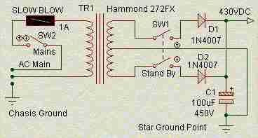 The raw voltage is generated by a Hammond 272FX transformer (372FX for our
Euro friends with 240V mains). The present circuit should look familiar to
tube amp folks. Filament windings are not shown (to be discussed later). The
HV secondary, 300-0-300VAC, is rectified by 1N4007 diodes to generate
~430VDC. C1, 100uF, provides the first filtering of the DC voltage. Solid
state rectifiers were chosen to get the maximum possible voltage.
The raw voltage is generated by a Hammond 272FX transformer (372FX for our
Euro friends with 240V mains). The present circuit should look familiar to
tube amp folks. Filament windings are not shown (to be discussed later). The
HV secondary, 300-0-300VAC, is rectified by 1N4007 diodes to generate
~430VDC. C1, 100uF, provides the first filtering of the DC voltage. Solid
state rectifiers were chosen to get the maximum possible voltage.Silicon diodes can supply large peak currents to recharge C1. 100uF was chosen to keep supply ripple in check. C1 is recharged every 8ms (120 times per second). The rated current is 150mA and C1 must supply that current between the recharge peaks from the diodes. C1 will charge to ~425V and then discharge for 8ms. We can calculate the amount of discharge.
Q = I * time
Q = 150mA * 8ms = 0.0012 Coulombs
V = Q / C
V = 0.0012 Coulombs / 100uF
V = 12V
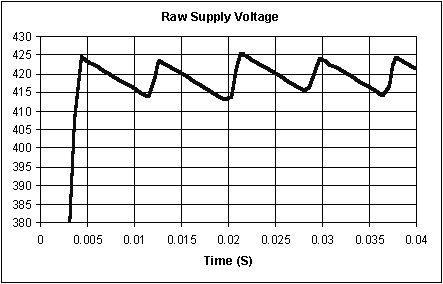 Thus, the supply voltage will drop from 425V to 413V between charges under full
load. A spice simulation (graph to left) shows what's happening. The raw
supply voltage charges up to 425V on the first peak from the tranny at 4ms.
The voltage decays to 413V in 8ms as C1 supplies 150mA to the load. C1 is
recharged to 425V at 12ms by the next peak from the tranny and the cycle
repeats. The minimum voltage of 413V is important in the following sections
covering voltage regulation. Don't use less than 100uF for C1!
Thus, the supply voltage will drop from 425V to 413V between charges under full
load. A spice simulation (graph to left) shows what's happening. The raw
supply voltage charges up to 425V on the first peak from the tranny at 4ms.
The voltage decays to 413V in 8ms as C1 supplies 150mA to the load. C1 is
recharged to 425V at 12ms by the next peak from the tranny and the cycle
repeats. The minimum voltage of 413V is important in the following sections
covering voltage regulation. Don't use less than 100uF for C1!Reference Voltage Source
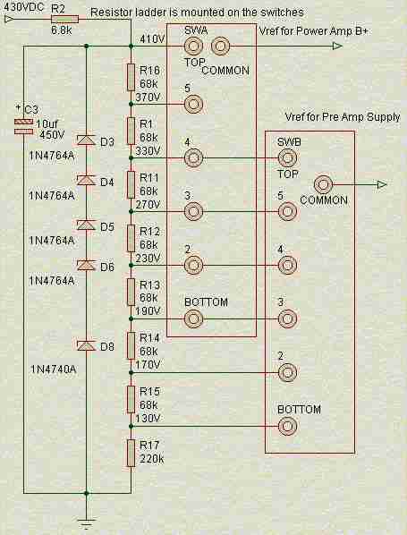 The PSM achieves voltage variability and regulation by first generating a
stable, clean reference voltage. A simple zener shunt regulator is used. The
zeners break down and conduct current at 410V. The top four diodes are 100V
and the bottom is 10V. R2 drops the raw voltage to 410V as the zeners draw
current. This voltage is filtered and used to supply a resistor divider that
chops up the 410V into 40V steps. 6-position switches then choose one of
those voltages to pass along to the MOSFET regulation devices.
The PSM achieves voltage variability and regulation by first generating a
stable, clean reference voltage. A simple zener shunt regulator is used. The
zeners break down and conduct current at 410V. The top four diodes are 100V
and the bottom is 10V. R2 drops the raw voltage to 410V as the zeners draw
current. This voltage is filtered and used to supply a resistor divider that
chops up the 410V into 40V steps. 6-position switches then choose one of
those voltages to pass along to the MOSFET regulation devices.The choice of R2 is not arbitrary. First, power dissipation in the zeners must be kept under 1W. Each zener drops 100V, so the max current is 10mA (P=VI, 1=100I, I=10mA). The max output voltage of the raw supply with no load is 450V. R2 must drop 40V supplying no more than 10mA. Thus, R2 must be at least 4K (V=IR, 40=0.01R, R=4K). Smaller values for R will overstress the zeners. 6.8K is chosen for a little guard band resulting in 6mA and ~600mW dissipation in the zeners.
 As the supply is loaded, the raw voltage drops. Ideally, the raw voltage must
stay above the zener voltage to maintain proper function. The zener voltage
will start to drop when the current in the zeners goes to zero, which
happens when the current in R2 drops to the level needed to maintain voltage
in the resistor divider. Adding up all the resistance in the divider gives
764K (8 times 68K plus 220K). To maintain 410V across the divider, 540uA
must be flowing (V=IR, 410=764K*I, I=540uA). 540uA through R2 is 3.7V (V=IR,
V=540uA*6.8K). Thus, if the raw supply drops below 413.7V (410+3.7) the
reference voltage will fall below 410V. Remember the minimum voltage we
calculated in the raw supply section above? That was 413V. So, we're on the
hairy edge of keeping the zener stack functioning under full load. This was
a conscious choice to get the maximum possible regulated voltage from the
PSM. Nothing is wasted!
As the supply is loaded, the raw voltage drops. Ideally, the raw voltage must
stay above the zener voltage to maintain proper function. The zener voltage
will start to drop when the current in the zeners goes to zero, which
happens when the current in R2 drops to the level needed to maintain voltage
in the resistor divider. Adding up all the resistance in the divider gives
764K (8 times 68K plus 220K). To maintain 410V across the divider, 540uA
must be flowing (V=IR, 410=764K*I, I=540uA). 540uA through R2 is 3.7V (V=IR,
V=540uA*6.8K). Thus, if the raw supply drops below 413.7V (410+3.7) the
reference voltage will fall below 410V. Remember the minimum voltage we
calculated in the raw supply section above? That was 413V. So, we're on the
hairy edge of keeping the zener stack functioning under full load. This was
a conscious choice to get the maximum possible regulated voltage from the
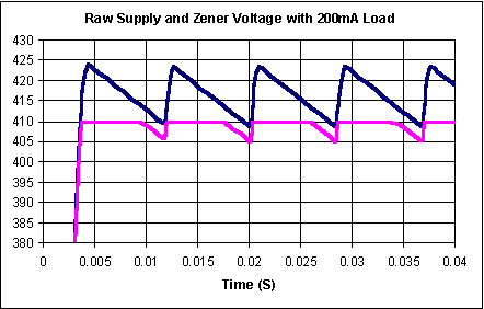
PSM. Nothing is wasted!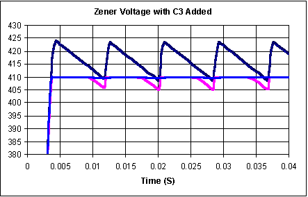 If the raw supply dips below 413V, the zener voltage will follow. Worse, the
zener voltage will also ripple as it follows the dips. This is bad because a
clean reference voltage is needed for regulation. The graph here shows the
zener voltage (purple) and the raw supply voltage when overloaded at 200mA.
As expected, when the raw supply drops below 413V, the zener voltage
follows. To ensure a clean reference voltage, C3 was added. Given that we
chose a zener voltage on the hairy edge, lower AC main voltage or perhaps
variation in different trannies will allow the raw supply to dip below 413V.
R2 and C3 form a low pass filter with a time constant of 50ms (t=RC,
t=6.8K*8uF, t=50ms). A time constant of 50ms means the voltage will take
50mS to move 63% of the way to some new target voltage. In fact, to make the
attached graphs, I had to cheat in the sim because the initial charging of
C3 takes ~150ms. C3 charges to 260V (63% of 410) in the first 50ms, then to
360V in the next 50mS (63% of the remaining 150V) and so on. In the sim, R2
is shorted for the first 4ms to force C3 to charge fast to 410V. The light
blue curve in the second graph shows the cleaned reference.
If the raw supply dips below 413V, the zener voltage will follow. Worse, the
zener voltage will also ripple as it follows the dips. This is bad because a
clean reference voltage is needed for regulation. The graph here shows the
zener voltage (purple) and the raw supply voltage when overloaded at 200mA.
As expected, when the raw supply drops below 413V, the zener voltage
follows. To ensure a clean reference voltage, C3 was added. Given that we
chose a zener voltage on the hairy edge, lower AC main voltage or perhaps
variation in different trannies will allow the raw supply to dip below 413V.
R2 and C3 form a low pass filter with a time constant of 50ms (t=RC,
t=6.8K*8uF, t=50ms). A time constant of 50ms means the voltage will take
50mS to move 63% of the way to some new target voltage. In fact, to make the
attached graphs, I had to cheat in the sim because the initial charging of
C3 takes ~150ms. C3 charges to 260V (63% of 410) in the first 50ms, then to
360V in the next 50mS (63% of the remaining 150V) and so on. In the sim, R2
is shorted for the first 4ms to force C3 to charge fast to 410V. The light
blue curve in the second graph shows the cleaned reference.Series Regulation
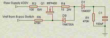
 The IRFP450 power MOSFET was chosen as the series regulation device. It's cheap
(under $3), can handle 500V and can dissipate 190W and is dirt simple to use
as a voltage regulator. The simplest possible regulator is simply a source
follower (very much like a cathode follower, if you're familiar with tube
circuits). The threshold voltage of the IRFP450 is 3V. A reference voltage
is applied to the gate and the FET will charge the cap until it shuts off.
The output voltage, with no load, will charge up to ~3V below the reference
voltage. The IRFP450 has a very high transconductance, designed to supply
many amps of current. For our tube supply, it only needs to supply 150mA.
Even under full load, the output voltage will remain near the no load case
(Vref minus 3V).
The IRFP450 power MOSFET was chosen as the series regulation device. It's cheap
(under $3), can handle 500V and can dissipate 190W and is dirt simple to use
as a voltage regulator. The simplest possible regulator is simply a source
follower (very much like a cathode follower, if you're familiar with tube
circuits). The threshold voltage of the IRFP450 is 3V. A reference voltage
is applied to the gate and the FET will charge the cap until it shuts off.
The output voltage, with no load, will charge up to ~3V below the reference
voltage. The IRFP450 has a very high transconductance, designed to supply
many amps of current. For our tube supply, it only needs to supply 150mA.
Even under full load, the output voltage will remain near the no load case
(Vref minus 3V).The key issues with this simple regulator are power dissipation and short circuit protection. In the case of a short circuit, the output voltage is zero while the gate voltage is still very high. The gate oxide is only rated for 30V, so we'll need to add a zener diode for protection between the gate and source. If the output is pulled to ground by a short, then the zener will pull the gate down to save the gate oxide. However, power dissipation still needs consideration. With a short circuit, the raw supply may remain up around 350V, supplying nearly an amp. That's 350W in the FET (P=VI=350*1), which would kill it in an instant. The FET essentially becomes a fuse. The addition of a current limiting resistor will save the FET. R4, 15 ohm in the next diagram, is the current sensing resistor. With no current, there's no drop across R4. Thus, the voltage across the 6.2V zener diode, D9, will only be 3V (the FET threshold voltage). However, when the load current reaches 200mA, R4 is dropping 3V. Add that to the FET threshold of 3V gives 6V across the zener, which is enough to start it conducting. If the load increases beyond 200mA, the zener will pull down on the gate and thus reduce the output voltage. The R4/D9 circuit essentially will not allow the FET to conduct more than 100mA. Under a short circuit condition, the current will rise to ~220mA.
 Power dissipation in the FET is then ~80W, which is reasonably safe. The original
goal was to achieve a circuit that can survive a short circuit indefinitely,
but this circuit doesn't quite make it.
Power dissipation in the FET is then ~80W, which is reasonably safe. The original
goal was to achieve a circuit that can survive a short circuit indefinitely,
but this circuit doesn't quite make it.Two FETs were sacrificed in the name of science! Under short circuit conditions, the FETs survived ~90s before blowing. At that point, they shorted out and blew the mains fuse. The final circuit includes a 200mA slow blow fuse (not shown in the present diagram) in the power amp B+ line to preserve the FET. DO NOT use a fuse rated higher than 200mA unless you like replacing FETs.
D1 is in series with the supply to prevent back flow of current from the output filter cap. In the event that Vref suddenly drops (when the user selects a lower voltage from the switch), the filter cap will discharge back through the reference supply. The original design used a potentiometer instead of a 6-pos switch, which promptly arced and fried when the filter cap forced it's voltage back through. D1 solved the problem. (More dead electronics lost to science.)
 R3 forms a pi filter between the raw supply filter cap and the output filter
cap, C1. This is needed to ensure a \clean supply under full load at the
highest voltage. Vref for the top voltage is 410V. We've already seen that
the raw supply dips down near this at 150mA load. R3 will drop another 15V.
As such, the regulator is simply passing the raw voltage, ripple and all.
The original design used a max ref voltage of 360V for a max regulated
output voltage of 350V to avoid this situation. But, there's no reason to
throw away 50V just to have perfect regulation. All the voltages below the
max will still be well regulated. The max voltage of 400V is still regulated
as well as normal tube supplies using a pi filter, so may as well make it
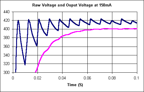
available. The adjacent plot shows the output voltage (purple) with a 150mA
DC load.
R3 forms a pi filter between the raw supply filter cap and the output filter
cap, C1. This is needed to ensure a \clean supply under full load at the
highest voltage. Vref for the top voltage is 410V. We've already seen that
the raw supply dips down near this at 150mA load. R3 will drop another 15V.
As such, the regulator is simply passing the raw voltage, ripple and all.
The original design used a max ref voltage of 360V for a max regulated
output voltage of 350V to avoid this situation. But, there's no reason to
throw away 50V just to have perfect regulation. All the voltages below the
max will still be well regulated. The max voltage of 400V is still regulated
as well as normal tube supplies using a pi filter, so may as well make it
available. The adjacent plot shows the output voltage (purple) with a 150mA
DC load.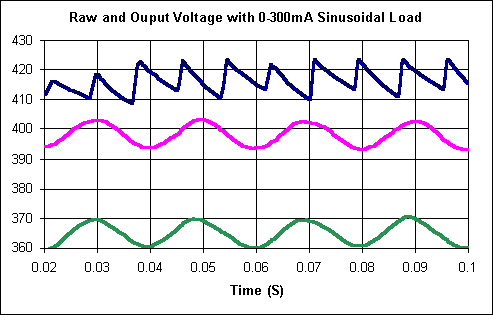 The next graph shows the output voltage with the worst-case AC loading. The
load is a 50hz sine wave of current ranging from 0 to 300mA (150mA average).
The purple and green lines are the output voltages with the max (400V) and
next (360V) selections, respectively. In each case, there's 10V of
"slop" in the output across the worst possible loading condition.
This is as good or better than the majority of B+ supplies used in tube amps.
The next graph shows the output voltage with the worst-case AC loading. The
load is a 50hz sine wave of current ranging from 0 to 300mA (150mA average).
The purple and green lines are the output voltages with the max (400V) and
next (360V) selections, respectively. In each case, there's 10V of
"slop" in the output across the worst possible loading condition.
This is as good or better than the majority of B+ supplies used in tube amps.Negative Voltage
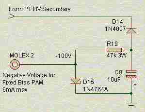 Negative voltage is generated from the same HV secondary as used for B+.
Simply connect a 1N4007 to either of the secondary leads to get
the negative voltage peaks, smooth them out with a filter cap and
shunt regulate with a zener diode. Note in the schematic that all
the components are "up side down" compared to a positive
supply. The filter cap + side is grounded. The cathode of the
zener is grounded and the cathode of the 1N4007 is at the tranny.
Negative voltage is generated from the same HV secondary as used for B+.
Simply connect a 1N4007 to either of the secondary leads to get
the negative voltage peaks, smooth them out with a filter cap and
shunt regulate with a zener diode. Note in the schematic that all
the components are "up side down" compared to a positive
supply. The filter cap + side is grounded. The cathode of the
zener is grounded and the cathode of the 1N4007 is at the tranny.Regulation is done the same way as the Vref supply used in the B+ circuits discussed earlier. The voltage on C8 is about -400V and R19 drops 300V. This means there is always ~6mA flowing in R19 (V=IR, 300=I*47k, I=6mA). R19 is chosen to keep the 1W, 100V zener from bloing out (P=VI=100*6mA=600mW). This also means that the bias circuit in the PAM (power amp module) can only draw 6mA, max. Beyond that, R19 will drop more than 300V and the negative voltage to the PAM won't be -100V.
Low Voltage 14VDC
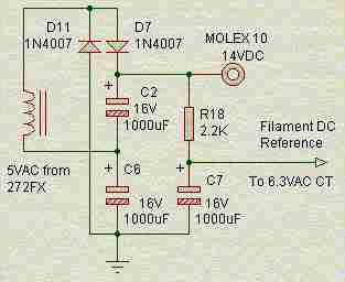 Since the Hammond 272FX has a 5VAC secondary, we may as well take
advantage. If you want channel switching using relays or maybe even some
solid sate circuits, low voltage DC is handy. A simple voltage doubler
gets 14VDC (~12V loaded). The peak voltage from the tranny is ~7V. The
positive peaks charge C2 to 7V through D7 and the negative peaks charge C6
to 7V through D11. C2 and C6 are connected in series to add their voltages
up to 14V for the output. Note that this is not regulated. If you want to
drive solid state audio circuitry, regulating down to 9 or 10V in your
circuit is advisable.
Since the Hammond 272FX has a 5VAC secondary, we may as well take
advantage. If you want channel switching using relays or maybe even some
solid sate circuits, low voltage DC is handy. A simple voltage doubler
gets 14VDC (~12V loaded). The peak voltage from the tranny is ~7V. The
positive peaks charge C2 to 7V through D7 and the negative peaks charge C6
to 7V through D11. C2 and C6 are connected in series to add their voltages
up to 14V for the output. Note that this is not regulated. If you want to
drive solid state audio circuitry, regulating down to 9 or 10V in your
circuit is advisable.