PSM Printed Circuit Boards...
Francisco Pena has done a great job making PCBs for the
AX84 Tone Brewery PSM.
You can find the PDF file of the PCB and parts layout at his site,
http://tonepad.com/.
But, why make your own when you can get one AT COST?! My cost was
$200 total for 16 boards and I'm selling for $13 plus shipping.
Figure $4 for US shipping. I'll ship outside the US but I have
no clue about the cost of shipping.
Of course, don't forget that I have 6x9x3 Chassis,
FETs, the heat sinks and maybe even a suitable PT!
I can set you up with all the stuff mouser doesn't have,
leaving you with just one order to place.
Or, I will also build you a fully assembled and tested PSM for $200.
Contents
 PSM PC Boards
Wiring
PSM PCBs
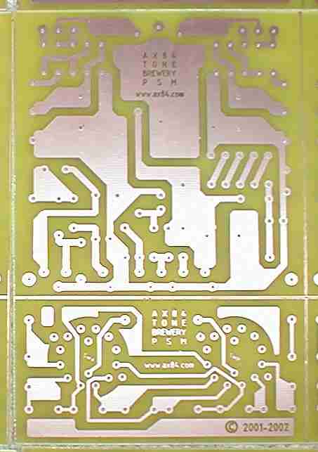
Here they are!! You actually get two for the price of one!!
Francisco did up a board for the rotary switches
along with the main PCB. You just cut off the switch board
and there you go! Have a look.
PCB Wiring
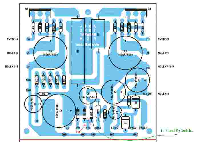
Here's the component layout showing the error needing corrected for the negative voltage.
Negative voltage should remain on during stand by to ensure the power tubes don't
draw excessive current coming out of stand by. I will fix the PCB before sending if you buy one.
You can find the PDF file of the PCB and parts layout at http://tonepad.com/.
The following is the guts of an email sent to Henry Ramsey to help him through his PCB wiring...
There's only one connection going to the switches and then one coming back from each switch to return the
reference level. The resistor ladder is mounted directly to the switches. The key thing here is to study
the schematic and then study the switch and don't solder anything until you fully understand and can "see"
in your mind exactly how the schematic and switches are linked. I tried to draw the schematic very much like
the actual switch wiring, physically, but I stopped short of making an actual picture of the switches. So,
get the schematic in front of you and I'll walk you through it.
The zener diode string is on the PCB. The resistor ladder next to it is on the switches. The node labeled
410V at the top of the zener stack is J7 on the PCB. This goes to the "top" of the High B+ Switch, SWA. The
"top" of the switch is the lug of the switch that is connected to the pole (or common) of the switch when it
is turned all the way up (full clock wise). So, grab a switch, turn it full clockwise, note which lug is now
connected to the pole and that's the top of the switch.
Now, the upper 5 resistors of the ladder, 16, 1, 11, 12 and 13, mount on SWA. They're all the same value, so
just grab a handful of 68K resistors and install them in sequence from the "top" to "bottom" on the lugs of
the switch. Don't solder them yet, however. Note on the schematic, you now need to run 4 wires from SWA
to SWB. SWB is the low B+ control. Add these 4 wires to SWA and then solder the lugs on SWA. By the way, I
suggest doing all this stuff to the switches before mounting them to the chassis. It's easier to wire them up,
then install them.
The last three resistors of the ladder mount to SWB. Note that R17 at the bottom of the stack is NOT 68K and
it's bottom goes to ground. Since the switches are double pole, you will have spare lugs on the switch for the
unused half. Mount one end of R17 to the bottom lug of SWB and mount the other end of R17 to one of those spare
lugs on SWB that isn't used by the circuit. A wire from this spare lug should then go back to the PCB to a gnd
point (the bottom of the zener stack). The PCB only shows one gnd hole. Feel free to drill extra holes near this
one, along the gnd buss, for additional gnd wires. You'll need 5 gnds to go to the Molex, 1 from the tranny CT
and 1 to go to SWB. The single gnd hole on the PCB is the star ground point of the whole system.
Finally, the pole (common) of the switches return to the PCB via a wire. The pole of SWA returns to J6 on the
PCB. The pole of SWB returns to J11 on the PCB.
The other tap points on the PCB are as follows:
HV1 HV secondary from tranny.
HV2 HV secondary from tranny.
GND HV CT from tranny.
BIAS -100V to Molex 2.
14V 12VDC to Molex 10.
5VAC1 5VAC from tranny.
5VAC2 5VAC from tranny.
J4 Raw B+. Not Used.
J5 High B+ to fuse 2 and then to Molex 12.
J6 SWA Pole (common).
J7 Top of Zener stack to SWA.
J8 Gnd of High B+ to Molex pins 4 & 5, using two separate wires.
J9 Low B+ to Molex 11.
J10 Gnd of Low B+ to Molex pins 7, 8 & 9 using three separate wires.
J11 SWB Pole (common).
J12 Tap from second zener. Not Used.
The remaining Molex pins are:
1 Chassis ground. Run a wire to a toothed washer bolted to the chassis.
3 6.3VAC from tranny.
6 6.3VAC from tranny.
